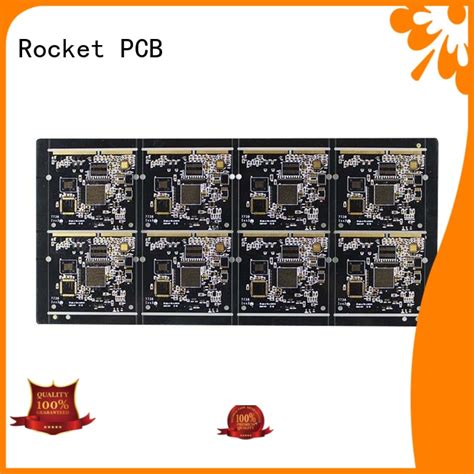
What are PCB Gold Fingers?
PCB gold fingers, also known as edge connectors or contact fingers, are the exposed metal pads on the edge of a printed circuit board (PCB) that facilitate electrical connections between the PCB and other components or devices. These gold-plated contacts are commonly found on computer memory modules, expansion cards, and various other electronic devices that require reliable and durable connections.
Advantages of PCB Gold Fingers
Gold is the preferred material for plating PCB fingers due to its exceptional properties:
- Excellent conductivity
- High resistance to corrosion and oxidation
- Durability and wear resistance
- Compatibility with lead-free soldering processes
PCB Gold Finger Plating Process
The process of applying gold plating to PCB fingers involves several steps to ensure a high-quality, reliable finish.
Step 1: PCB Fabrication
Before the gold plating process can begin, the PCB must be fabricated according to the design specifications. This includes:
- Substrate selection (e.g., FR-4, polyimide)
- Copper foil lamination
- Drilling and routing
- Copper pattern etching
Step 2: Surface Preparation
To ensure proper adhesion of the gold plating, the PCB surface must be thoroughly cleaned and prepared:
- Degreasing to remove oils and contaminants
- Micro-etching to roughen the surface for better adhesion
- Acid cleaning to remove oxides and activate the surface
Step 3: Nickel Plating
A layer of nickel is plated onto the copper fingers to serve as a barrier and promote adhesion of the gold layer:
- Electroless nickel plating (ENIG) or electrolytic nickel plating
- Typical nickel thickness: 2-5 µm
Step 4: Gold Plating
The final step involves plating a layer of gold onto the nickel-plated fingers:
- Electroplating or immersion plating
- Typical gold thickness: 0.05-2 µm (depending on application requirements)
| Application | Typical Gold Thickness |
|---|---|
| Edge connectors | 0.2-1.0 µm |
| High-reliability connectors | 1.0-2.0 µm |
| Decorative purposes | 0.05-0.2 µm |
Step 5: Quality Control
After gold plating, the PCBs undergo rigorous quality control checks to ensure they meet the required specifications:
- Visual inspection for surface defects and uniformity
- Thickness measurement using X-ray fluorescence (XRF) or cross-sectioning
- Adhesion testing (tape test or peel test)
- Solderability testing
PCB Gold Finger Design Considerations
When designing PCBs with gold fingers, several factors must be taken into account:
Finger Dimensions
The dimensions of the gold fingers (width, length, and pitch) should be designed according to the mating connector specifications and industry standards (e.g., PCI, PCIe, DIMM).
Copper Thickness
The underlying copper thickness of the fingers should be sufficient to ensure mechanical strength and current-carrying capacity. Typical copper thicknesses range from 17.5 µm (0.5 oz) to 70 µm (2 oz).
Solder Mask Opening
The solder mask opening around the gold fingers should be designed to provide adequate clearance for the mating connector while maintaining a proper seal to prevent contamination.
Surface Finish
In addition to gold plating, other surface finishes can be used for PCB fingers, such as:
- Immersion tin (ISn)
- Immersion silver (IAg)
- Organic solderability preservative (OSP)
The choice of surface finish depends on the specific application requirements, cost considerations, and compatibility with the assembly process.

Frequently Asked Questions (FAQ)
1. What is the difference between hard and soft gold plating?
Hard gold plating contains a small percentage of cobalt or nickel to increase its hardness and wear resistance. It is typically used for high-wear applications, such as edge connectors or test probes. Soft gold plating, on the other hand, is pure gold and is more ductile, making it suitable for applications requiring flexibility or wire bonding.
2. Can gold fingers be repaired if damaged?
In some cases, damaged gold fingers can be repaired using a process called “gold finger rework.” This involves removing the damaged gold plating, preparing the surface, and re-plating the fingers with gold. However, the success of the repair depends on the extent of the damage and the skill of the technician performing the rework.
3. How does the thickness of the gold plating affect performance?
Thicker gold plating generally provides better wear resistance and longer-lasting protection against corrosion. However, excessive gold thickness can lead to issues such as embrittlement, reduced flexibility, and increased cost. The optimal gold thickness depends on the specific application requirements and should be determined based on factors such as the expected number of mating cycles, environmental conditions, and cost constraints.
4. Can gold fingers be used in high-frequency applications?
Yes, gold fingers can be used in high-frequency applications due to gold’s excellent electrical conductivity and resistance to oxidation. However, in high-frequency PCB designs, special considerations must be taken to ensure proper impedance matching, signal integrity, and EMI/EMC compliance. This may involve optimizing the finger geometry, spacing, and surrounding PCB layout to minimize signal reflections and crosstalk.
5. How do I specify gold finger plating requirements to my PCB manufacturer?
When ordering PCBs with gold fingers, it is essential to communicate your plating requirements clearly to your PCB manufacturer. This typically involves specifying the following:
- Gold plating thickness (in micrometers)
- Plating type (hard or soft gold)
- Underlying nickel plating thickness and type (if applicable)
- Finger dimensions and tolerances
- Any additional requirements, such as surface roughness or specific industry standards to be met
Providing clear and detailed specifications helps ensure that your PCB manufacturer can deliver gold fingers that meet your exact requirements and performance expectations.
Conclusion
PCB gold fingers play a crucial role in ensuring reliable and durable electrical connections in a wide range of electronic devices. By understanding the gold plating process, design considerations, and key factors affecting performance, engineers and technicians can make informed decisions when specifying and working with gold-plated PCBs. As technology continues to advance, the demand for high-quality, reliable gold fingers will only continue to grow, making it essential for professionals in the electronics industry to stay up-to-date with the latest developments and best practices in PCB gold finger plating.

No responses yet