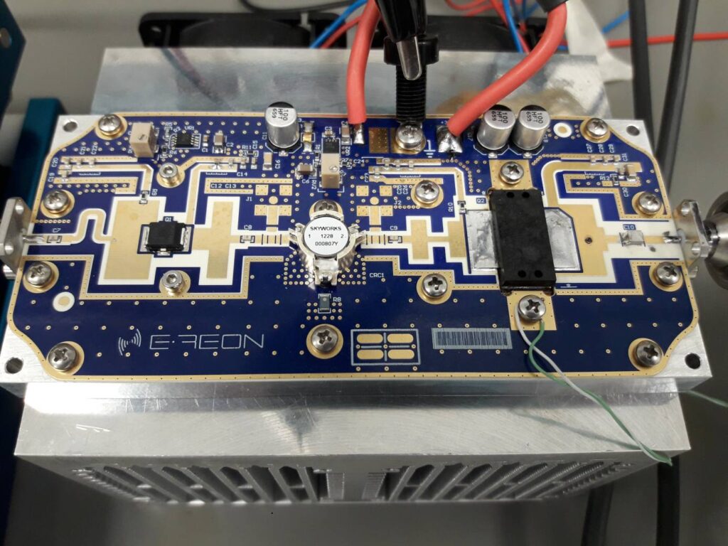
In the realm of high-frequency and mixed-signal circuit design, the layout of the printed circuit board (PCB) plays a crucial role in ensuring optimal performance, signal integrity, and reliability. Radio frequency (RF) and mixed-signal circuits are particularly sensitive to layout considerations due to their inherent complexity and susceptibility to various parasitic effects. Adhering to proper PCB layout guidelines is essential to mitigate these challenges and achieve the desired functionality. In this article, we will explore key PCB layout guidelines for RF and mixed-signal designs, covering essential aspects such as grounding, routing, component placement, and more.
Understanding RF and Mixed-Signal Design Challenges
RF and mixed-signal circuits operate at high frequencies, often involving both analog and digital components. These designs are inherently prone to several challenges, including:
- Signal Integrity: High-frequency signals are susceptible to various forms of interference, such as crosstalk, reflections, and electromagnetic interference (EMI). Ensuring signal integrity is crucial for reliable data transmission and overall circuit performance.
- Power Integrity: The coexistence of analog and digital components in mixed-signal designs can lead to power supply noise, ground bounce, and other power integrity issues, affecting circuit operation and potentially causing malfunctions.
- Electromagnetic Compatibility (EMC): RF and mixed-signal circuits can both generate and be susceptible to electromagnetic interference, necessitating careful EMC considerations during the design and layout process.
- Parasitic Effects: At high frequencies, parasitic capacitances, inductances, and resistances can significantly impact circuit behavior, potentially causing unwanted resonances, signal distortion, and losses.
Adhering to proper PCB layout guidelines is essential to address these challenges and ensure optimal circuit performance.
Grounding Strategies
Proper grounding is fundamental in RF and mixed-signal designs, as it plays a crucial role in ensuring signal integrity, power integrity, and EMC compliance.
Ground Planes
- Use solid ground planes: Solid ground planes provide a low-impedance return path for high-frequency signals, reducing loop inductance and minimizing ground bounce and EMI issues.
- Separate analog and digital ground planes: Isolate analog and digital ground planes to prevent noise coupling between the two domains. Connect the analog and digital ground planes at a single point, known as the “star ground” or “ground via stitching.”
- Avoid ground plane splits and discontinuities: Splits and discontinuities in the ground plane can create impedance discontinuities and potential return path issues, leading to signal reflections and EMI problems.
Ground Vias
- Use multiple ground vias for connection: Use multiple ground vias to provide a low-impedance path between the ground planes and the component ground pins, minimizing ground loops and ensuring proper return paths.
- Place ground vias close to signal paths: Position ground vias in close proximity to high-frequency signal paths, providing a low-inductance return path and minimizing loop areas.
- Use via stitching for multi-layer designs: In multi-layer PCBs, use via stitching to create a continuous ground reference between layers, ensuring a robust ground connection throughout the board.
Signal Routing
Proper signal routing is crucial for maintaining signal integrity and minimizing electromagnetic interference in RF and mixed-signal designs.
Trace Considerations
- Controlled impedance routing: Use controlled impedance routing techniques, such as microstrip or stripline configurations, to match the characteristic impedance of the transmission lines to the desired value (e.g., 50 ohms).
- Minimize trace lengths: Keep trace lengths as short as possible to reduce propagation delays, signal reflections, and radiated emissions.
- Avoid right-angle bends: Use curved or mitered bends instead of right-angle bends to minimize impedance discontinuities and signal reflections.
- Maintain spacing between traces: Maintain adequate spacing between traces to minimize crosstalk and electromagnetic coupling.
- Use differential pair routing: For differential signaling, route the differential pairs with consistent spacing and length matching to maintain signal integrity and common-mode rejection.
Shielding and Isolation
- Isolate sensitive traces: Route sensitive analog and RF traces away from noisy digital signals to minimize interference and crosstalk.
- Use grounded guard rings: Surround sensitive analog and RF components with grounded guard rings or ground planes to provide shielding and isolation from external interference.
- Consider using shielded vias: In multi-layer designs, use shielded vias (also known as “stitched vias”) to provide isolation between signal layers and minimize crosstalk and EMI.
Component Placement
Proper component placement is essential for minimizing parasitic effects, reducing electromagnetic interference, and ensuring efficient power distribution in RF and mixed-signal designs.
- Partition the board: Partition the board into separate analog, digital, and RF sections, isolating sensitive components from potential sources of interference.
- Minimize trace lengths: Place components in a manner that minimizes trace lengths, especially for high-frequency signals, to reduce propagation delays and signal reflections.
- Maintain symmetry: For differential signaling, maintain symmetry in the placement of components and routing to ensure balanced propagation delays and common-mode rejection.
- Avoid ground loops: Arrange components and routing to minimize ground loops, which can introduce noise and electromagnetic interference.
- Consider thermal management: Place high-power components strategically to facilitate efficient heat dissipation and avoid thermal stress on sensitive components.
Power Distribution
Proper power distribution is crucial for maintaining power integrity and minimizing noise in RF and mixed-signal designs.
- Use separate power planes: Separate power planes for analog, digital, and RF sections to prevent noise coupling and maintain isolation.
- Decoupling capacitors: Use appropriate decoupling capacitors near power pins of sensitive components to provide local bypass capacitance and minimize power supply noise.
- Bypass capacitor placement: Place bypass capacitors as close as possible to the power and ground pins of the components they are decoupling, minimizing parasitic inductance and ensuring effective decoupling.
- Power distribution networks: Design power distribution networks with low impedance and minimal inductance to ensure clean power delivery and minimize ground bounce.
- Ferrite beads and filtering: Use ferrite beads or filtering components on power and signal lines to suppress high-frequency noise and prevent interference coupling.
EMC Considerations

Electromagnetic compatibility (EMC) is a critical aspect of RF and mixed-signal designs, as these circuits can both generate and be susceptible to electromagnetic interference.
- Shielding: Use appropriate shielding techniques, such as metal enclosures or shielded cables, to contain electromagnetic emissions and protect sensitive circuits from external interference.
- Filter inputs and outputs: Implement filtering on input and output lines to suppress conducted emissions and prevent external interference from entering the circuit.
- Grounding and bonding: Ensure proper grounding and bonding practices, including the use of low-impedance ground connections and minimizing ground loops, to mitigate EMI issues.
- Layout optimization: Optimize the PCB layout by following the guidelines outlined in this article, such as proper grounding, signal routing, and component placement, to minimize electromagnetic emissions and susceptibility.
- EMC testing and compliance: Conduct thorough EMC testing and ensure compliance with relevant standards and regulations for your target application and region.
Comparison Table: Key Layout Considerations
To summarize the key layout considerations for RF and mixed-signal designs, we’ve provided a comprehensive table:
| Layout Aspect | Considerations |
|---|---|
| Grounding | – Use solid ground planes <br> – Separate analog and digital ground planes <br> – Avoid ground plane splits and discontinuities <br> – Use multiple ground vias for connection <br> – Place ground vias close to signal paths <br> – Use via stitching for multi-layer designs |
| Signal Routing | – Controlled impedance routing <br> – Minimize trace lengths <br> – Avoid right-angle bends <br> – Maintain spacing between traces <br> – Use differential pair routing <br> – Isolate sensitive traces <br> – Use grounded guard rings <br> – Consider using shielded vias |
| Component Placement | – Partition the board <br> – Minimize trace lengths <br> – Maintain symmetry for differential signaling <br> – Avoid ground loops <br> – Consider thermal management |
| Power Distribution | – Use separate power planes <br> – Use decoupling capacitors <br> – Proper bypass capacitor placement <br> – Design low-impedance power distribution networks <br> – Use ferrite beads and filtering |
| EMC Considerations | – Shielding <br> – Filter inputs and outputs <br> – Grounding and bonding <br> – Layout optimization <br> – EMC testing and compliance |
Frequently Asked Questions (FAQs)
- Why is controlled impedance routing important in RF and mixed-signal designs? Controlled impedance routing ensures that the characteristic impedance of the transmission lines matches the desired value (e.g., 50 ohms). This minimizes signal reflections, ensures proper signal propagation, and maintains signal integrity at high frequencies.
- What is the purpose of separating analog and digital ground planes? Separating analog and digital ground planes prevents noise coupling between the two domains. Digital circuits can introduce significant noise on the ground plane, which can adversely affect the performance of sensitive analog circuits if they share the same ground plane.
- How do grounded guard rings help in RF and mixed-signal designs? Grounded guard rings provide shielding and isolation for sensitive analog and RF components. By surrounding these components with a grounded ring or ground plane, external interference and crosstalk are minimized, improving signal integrity and overall circuit performance.
- Why is it important to minimize trace lengths in RF and mixed-signal designs? Minimizing trace lengths reduces propagation delays, signal reflections, and radiated emissions. Longer traces act as antennas, increasing the susceptibility to electromagnetic interference and potentially causing signal integrity issues at high frequencies.
- What is the significance of proper bypass capacitor placement in RF and mixed-signal designs? Proper bypass capacitor placement is crucial for effective decoupling and minimizing power supply noise. Bypass capacitors should be placed as close as possible to the power and ground pins of the components they are decoupling to minimize parasitic inductance and ensure efficient decoupling at high frequencies.
By following these PCB layout guidelines for RF and mixed-signal designs, engineers can mitigate various challenges, ensure signal integrity, maintain power integrity, and achieve reliable and robust circuit performance. Adherence to these practices is essential for successful design and implementation of high-frequency and mixed-signal circuits.
No responses yet