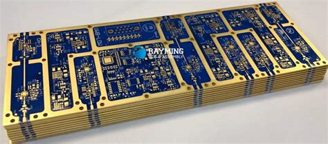
Why is PCB Edge Clearance Important?
Edge clearance is crucial for several reasons:
-
Manufacturing processes: During PCB fabrication, boards undergo various processes like drilling, routing, and depaneling. Adequate edge clearance prevents damage to components and traces near the board edges.
-
Mechanical stability: Components placed too close to the edges are susceptible to mechanical stress, vibration, and impact, which can cause cracks, disconnections, or complete component detachment.
-
Electrical integrity: Insufficient edge clearance can lead to short circuits, signal integrity issues, and electromagnetic interference (EMI) problems, especially in high-frequency or high-speed designs.
-
Assembly and handling: Proper edge clearance facilitates smooth assembly processes, such as pick-and-place, soldering, and testing, while also allowing for easier handling during production and use.
Industry Standards for PCB Edge Clearance
Various industry standards and guidelines provide recommendations for minimum edge clearance distances. Some widely recognized standards include:
- IPC-2221: Generic Standard on Printed Board Design
- IPC-7351: Generic Requirements for Surface Mount Design and Land Pattern Standard
- IPC-6012: Qualification and Performance Specification for Rigid Printed Boards
These standards offer general guidance, but specific requirements may vary depending on the PCB manufacturer, material, thickness, and application. Always consult with your manufacturer for their recommended edge clearance specifications.
Here’s a table summarizing some typical minimum edge clearance values based on IPC-2221:
| PCB thickness | Minimum Edge Clearance |
|---|---|
| <1.6 mm | 0.5 mm |
| 1.6 – 2.4 mm | 0.75 mm |
| >2.4 mm | 1.0 mm |
Best Practices for Maintaining Proper Edge Clearance
To ensure your PCB design adheres to edge clearance guidelines, follow these best practices:
1. Plan your component placement
Start by placing components at least the minimum required distance from the board edges. Group components logically and consider their sizes, heights, and power dissipation requirements.
2. Route traces carefully
When routing traces, maintain the specified clearance from the board edges. Avoid running traces parallel to the edges for long distances, as this increases the risk of damage during manufacturing.
3. Use keep-out zones
Define keep-out zones in your CAD tools to create visual boundaries for component placement and trace routing. These zones help you maintain edge clearance and avoid design rule violations.
4. Consider panelization
If your design will be panelized for production, account for additional clearance between individual boards and the panel edges. Consult with your manufacturer for their specific panelization requirements.
5. Perform design rule checks (DRC)
Utilize the DRC features in your PCB design software to verify that your design meets edge clearance requirements. Set up custom rules based on your manufacturer’s specifications and run DRC regularly during the design process.

Strategies for Optimizing Edge Clearance
In some cases, you may need to optimize your design to accommodate edge clearance requirements while still meeting functionality and size constraints. Here are a few strategies to consider:
-
Use smaller components: Select smaller form factors, such as chip-scale packages (CSPs) or micro-BGAs, to reduce the overall footprint and provide more space near the board edges.
-
Employ high-density interconnect (HDI) techniques: HDI PCBs use smaller vias, finer trace widths, and multiple layers to pack more functionality into a smaller area. This can help maintain edge clearance while still achieving the required functionality.
-
Optimize component orientation: Experiment with different component orientations to find the most space-efficient layout. Rotating components can sometimes provide better clearance without compromising performance.
-
Consider alternative board shapes: If your design allows, explore non-rectangular board shapes that can better accommodate component placement and edge clearance requirements.
FAQ
1. What happens if I don’t follow edge clearance guidelines?
Failing to maintain proper edge clearance can lead to manufacturing issues, such as drill breakout, trace damage, or component misalignment. It can also cause reliability problems in the field, like component detachment or short circuits due to mechanical stress or vibration.
2. Can I use smaller edge clearances than the recommended values?
While it’s generally not advisable to use smaller edge clearances than the recommended values, there may be situations where it’s necessary due to size constraints or other design requirements. In such cases, consult with your PCB manufacturer to discuss the feasibility and any potential risks or trade-offs.
3. What if my components are taller than the edge clearance distance?
If your components are taller than the edge clearance distance, you may need to consider alternative component placement or board layout strategies. One option is to place taller components closer to the center of the board, away from the edges. Another approach is to use a larger board size to accommodate the required clearances.
4. How do I ensure my design meets edge clearance requirements?
To ensure your design meets edge clearance requirements, follow best practices such as planning component placement, routing traces carefully, using keep-out zones, and performing design rule checks (DRC) in your PCB design software. Collaborate closely with your PCB manufacturer and adhere to their specific guidelines and recommendations.
5. Are there any exceptions to edge clearance rules?
In some cases, there may be exceptions to standard edge clearance rules. For example, certain connectors or mechanical features may require specific clearances that differ from the general guidelines. Always refer to the manufacturer’s datasheets and consult with your PCB manufacturer for guidance on any special requirements or exceptions.
Conclusion
Maintaining proper PCB edge clearance is essential for ensuring the manufacturability, reliability, and functionality of your circuit boards. By understanding the importance of edge clearance, adhering to industry standards, and following best practices, you can create designs that are optimized for production and long-term performance. Remember to collaborate closely with your PCB manufacturer, leverage the tools and features in your design software, and be open to alternative strategies when necessary. With careful planning and attention to detail, you can successfully navigate the challenges of edge clearance and create high-quality, reliable PCBs.

No responses yet