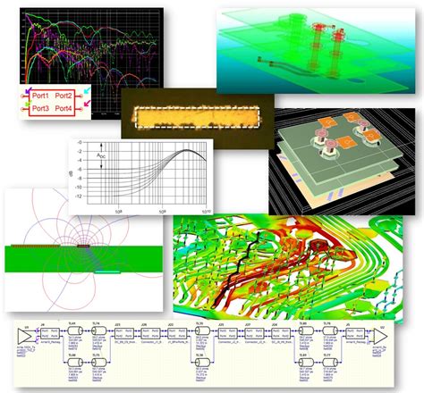
Introduction to PCB Simulation
Printed circuit board (PCB) simulation is the process of using computer-aided design (CAD) software to model, analyze, and verify the performance of a PCB design before it is manufactured. PCB simulation allows engineers to identify and fix potential issues early in the design process, reducing the risk of costly redesigns and production delays.
There are two main types of PCB simulation: pre-layout simulation and post-layout simulation. Each type focuses on different aspects of the PCB design and provides valuable insights into its functionality, reliability, and manufacturability.
Pre-Layout PCB Simulation
Pre-layout PCB simulation, also known as schematic-level simulation, is performed before the physical layout of the PCB is created. This type of simulation focuses on the electrical behavior of the circuit, including component values, interconnections, and signal integrity.
Objectives of Pre-Layout Simulation
The main objectives of pre-layout PCB simulation are:
- Verifying the logical functionality of the circuit
- Optimizing component values and tolerances
- Analyzing power consumption and thermal performance
- Assessing signal integrity and identifying potential issues, such as crosstalk and reflections
Tools and Techniques for Pre-Layout Simulation
Several tools and techniques are used for pre-layout PCB simulation, including:
- SPICE (Simulation Program with Integrated Circuit Emphasis) simulators
- Behavioral models for complex components, such as microcontrollers and digital signal processors
- Frequency-domain analysis for assessing the frequency response of the circuit
- Time-domain analysis for evaluating transient behavior and signal integrity
Benefits of Pre-Layout Simulation
Pre-layout PCB simulation offers several benefits, such as:
- Early identification and correction of design errors
- Reduced risk of costly redesigns and production delays
- Improved circuit performance and reliability
- Faster time-to-market for the final product
Post-Layout PCB Simulation
Post-layout PCB simulation is performed after the physical layout of the PCB has been created. This type of simulation considers the actual geometry and placement of components, traces, and vias, as well as the electrical properties of the materials used in the PCB.
Objectives of Post-Layout Simulation
The main objectives of post-layout PCB simulation are:
- Verifying the performance of the PCB design in a realistic environment
- Assessing the impact of the physical layout on signal integrity and electromagnetic compatibility (EMC)
- Identifying and mitigating issues related to parasitics, such as capacitance and inductance
- Optimizing the layout for manufacturability and reliability
Tools and Techniques for Post-Layout Simulation
Several tools and techniques are used for post-layout PCB simulation, including:
- Electromagnetic field solvers for analyzing the interactions between components and traces
- Finite element analysis (FEA) for evaluating thermal and mechanical stress
- 3D modeling and visualization for assessing the physical layout and identifying potential issues
- Design rule checking (DRC) for verifying compliance with manufacturing constraints
Benefits of Post-Layout Simulation
Post-layout PCB simulation offers several benefits, such as:
- Improved signal integrity and EMC performance
- Reduced risk of manufacturing defects and reliability issues
- Optimized layout for better thermal management and mechanical stability
- Faster and more cost-effective prototyping and production

Comparing Pre-Layout and Post-Layout PCB Simulation
While both pre-layout and post-layout PCB simulations are essential for designing high-quality PCBs, they differ in several key aspects, as summarized in the table below:
| Aspect | Pre-Layout Simulation | Post-Layout Simulation |
|---|---|---|
| Focus | Electrical behavior | Physical layout |
| Objectives | Verifying functionality, optimizing components, analyzing signal integrity | Assessing layout impact, identifying parasitics, optimizing manufacturability |
| Tools | SPICE simulators, behavioral models, frequency/time-domain analysis | Electromagnetic field solvers, FEA, 3D modeling, DRC |
| Benefits | Early error detection, improved performance, faster time-to-market | Better signal integrity and EMC, reduced manufacturing risks, optimized layout |
Best Practices for Effective PCB Simulation
To ensure the success of your PCB design project, consider the following best practices for effective simulation:
- Start with pre-layout simulation to verify the circuit’s functionality and optimize components
- Use accurate models and libraries for components and materials
- Perform post-layout simulation to assess the impact of the physical layout on performance
- Iterate between pre-layout and post-layout simulations to refine the design
- Validate simulation results with physical prototypes and testing
FAQ
1. What is the main difference between pre-layout and post-layout PCB simulation?
Pre-layout simulation focuses on the electrical behavior of the circuit, while post-layout simulation considers the physical layout and its impact on performance.
2. Can I skip pre-layout simulation and go straight to post-layout simulation?
While it is possible to skip pre-layout simulation, it is not recommended. Pre-layout simulation helps identify and correct design errors early, reducing the risk of costly redesigns and delays.
3. What are the most common tools used for PCB simulation?
SPICE simulators, electromagnetic field solvers, finite element analysis (FEA) tools, and 3D modeling software are among the most common tools used for PCB simulation.
4. How can PCB simulation help reduce manufacturing costs?
PCB simulation can help identify and mitigate potential manufacturing issues, such as design rule violations and reliability concerns, before the PCB is sent for production. This reduces the risk of costly rework and delays.
5. Is PCB simulation a substitute for physical prototyping and testing?
No, PCB simulation is not a substitute for physical prototyping and testing. While simulation can provide valuable insights and help optimize the design, it is essential to validate the results with real-world testing to ensure the PCB meets all performance and reliability requirements.
Conclusion
PCB simulation is a critical process in the design and development of high-quality printed circuit boards. By understanding the differences between pre-layout and post-layout simulation, and leveraging the appropriate tools and techniques, engineers can create PCBs that are functionally sound, reliable, and manufacturable.
Effective PCB simulation involves a combination of pre-layout and post-layout analyses, as well as adherence to best practices and validation through physical prototyping and testing. By investing in comprehensive PCB simulation, companies can reduce development costs, improve product quality, and accelerate time-to-market for their electronic devices.

No responses yet