1. Incorrect Layer Naming and File Extensions
One of the most frequent Gerber File Mistakes is using incorrect layer names and file extensions. This can cause confusion and delays in the manufacturing process.
How to Avoid This Mistake:
- Use standardized Gerber file extensions (e.g., .gbr, .top, .bot, .smt)
- Clearly name each layer according to its function (e.g., Top_Layer.gbr, Bottom_Layer.gbr, Solder_Mask_Top.gbr)
- Include a README file or Gerber file description to explain the layer naming convention
| Correct Gerber File Name | Incorrect Gerber File Name |
|---|---|
| Top_Layer.gbr | Layer1.gbr |
| Bottom_Layer.gbr | Layer2.gbr |
| Solder_Mask_Top.gbr | Top_Mask.gbr |
2. Missing or Incorrect Drill Files
Drill files are essential for specifying the location and size of holes in the PCB. Failing to include drill files or providing incorrect drill information can result in manufacturing issues.
How to Avoid This Mistake:
- Always include drill files (e.g., .drl, .txt) with your Gerber files
- Ensure drill files are generated in the correct format (e.g., Excellon)
- Double-check the drill sizes and locations before submitting files for manufacturing
3. Incorrect Aperture Definitions
Aperture definitions specify the shapes and sizes used in the Gerber files. Incorrect aperture definitions can lead to missing or distorted features on the manufactured PCB.
How to Avoid This Mistake:
- Use a consistent aperture list across all Gerber files
- Verify that the aperture sizes and shapes match the design intent
- Include an aperture list file (e.g., .rep) with your Gerber files

4. Overlapping or Conflicting Traces and Pads
Overlapping or conflicting traces and pads can cause short circuits and other manufacturing issues.
How to Avoid This Mistake:
- Perform a design rule check (DRC) to identify and resolve overlapping or conflicting features
- Ensure adequate spacing between traces and pads based on the PCB manufacturer’s guidelines
- Review the Gerber files carefully to verify that no overlaps or conflicts exist
5. Incorrect Board Outline and Dimensions
An incorrect board outline or dimensions can result in a PCB that does not fit the intended enclosure or fails to meet the desired specifications.
How to Avoid This Mistake:
- Include a clearly defined board outline layer in your Gerber files
- Double-check the board dimensions against the design requirements
- Verify that the board outline matches the mechanical drawings or 3D models
6. Missing or Incorrect Solder Mask and Silkscreen Files
Solder mask and silkscreen files are crucial for protecting the PCB and providing useful information for assembly and debugging. Missing or incorrect files can lead to manufacturing issues and difficulty in assembling the PCB.
How to Avoid This Mistake:
- Include solder mask and silkscreen files in your Gerber file package
- Ensure the solder mask and silkscreen apertures are correctly defined
- Verify that the solder mask and silkscreen layers align with the copper layers and board outline
7. Incomplete or Inconsistent Gerber File Package
An incomplete or inconsistent Gerber file package can cause delays in the manufacturing process and may result in a PCB that does not meet the design intent.
How to Avoid This Mistake:
- Use a Gerber file checklist to ensure all necessary files are included
- Verify that all files are generated from the same CAD database and version
- Include a README file or Gerber file description to explain the contents of the file package
By avoiding these common Gerber file mistakes, you can streamline the PCB manufacturing process, reduce costs, and ensure a high-quality end product.
FAQ
1. What are Gerber files?
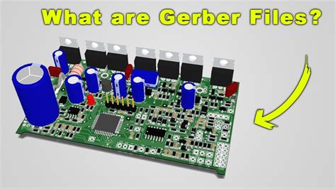
Gerber files are a standard format used to describe the printed circuit board (PCB) layers and manufacturing information needed for PCB fabrication. They contain data on copper layers, solder mask, silkscreen, drill holes, and board outline.
2. What happens if I submit Gerber files with mistakes?
Submitting Gerber files with mistakes can lead to manufacturing issues, delays, and added costs. The PCB manufacturer may need to contact you for clarification or request updated files, which can prolong the manufacturing process.
3. How can I ensure my Gerber files are error-free?
To ensure your Gerber files are error-free, follow these best practices:
- Use a consistent naming convention and file extensions
- Perform a design rule check (DRC) before generating Gerber files
- Carefully review the generated Gerber files for errors or discrepancies
- Use a Gerber file viewer to visually inspect the files
- Include a README file or Gerber file description to clarify the file contents
4. What should I do if I discover a mistake in my Gerber files after submitting them for manufacturing?
If you discover a mistake in your Gerber files after submitting them for manufacturing, contact your PCB manufacturer immediately. Provide the correct files and clearly explain the changes made. The sooner you address the issue, the less impact it will have on the manufacturing process.
5. Can PCB manufacturers modify my Gerber files to correct mistakes?
While some PCB manufacturers may be able to make minor modifications to your Gerber files, it is not recommended to rely on this. It is always best to submit error-free Gerber files to avoid any miscommunication or unintended changes to your design.
By understanding and avoiding these common Gerber file mistakes, you can work more effectively with your PCB manufacturer, like RAYPCB, to ensure a smooth and successful PCB fabrication process. Remember to carefully review your files, use consistent naming conventions, and include all necessary information to minimize the risk of manufacturing issues and delays.

No responses yet